- 您现在的位置:买卖IC网 > Sheet目录39249 > LM4867LQ/NOPB (NATIONAL SEMICONDUCTOR CORP) 3 W, 2 CHANNEL, AUDIO AMPLIFIER, PQCC24
Application Information (Continued)
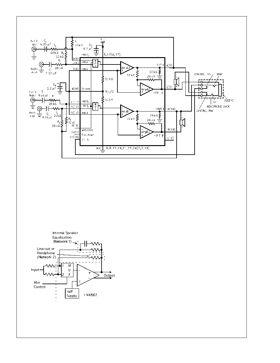
STEREO-INPUT MULTIPLEXER (STEREO MUX)
The LM4867 has two stereo inputs. The MUX CTRL Pin
controls which stereo input is active. As shown in the Truth
Table for Logic Inputs, applying 0V to the MUX CTRL input
activates stereo input 1, whereas applying V
DD to the MUX
CTRL inputs activates stereo input 2. To ensure correct
amplifier operation, unused MUX inputs must be tied to
GND.
Typical LM4867 applications use the MUX to switch between
two stereo input signals. Each stereo channel’s gain can be
tailored to produce the required output signal level by choos-
ing the appropriate input and feedback resistor ratio.
Another configuration uses the MUX to select two different
gains or frequency compensated gains that amplify a single
pair of stereo input signals. Figure 5 shows two different
feedback networks, Network 1 and Network 2. Network 1
produces increasing gain as the input signal’s frequency
decreases. This can be used to compensate a small, full-
range speaker’s low frequency response roll-off. Network 2
sets the gain for an alternate load such as headphones. The
circuit in Figure 6 uses Network 1 when driving external
speakers, switching to Network 2 when headphones are
connected. The normally closed control switch in Figure 6’s
headphone jack connects to the MUX CTRL pin. When
headphones are connected, the LM4867’s internal pull-up
that applies V
DD to the HP-IN and the external 100k
resis-
tor applies V
DD to MUX CTRL pin. Simultaneously applying
these control voltages automatically selects the amplifier
(headphone or bridge) and switches the gain (MUX channel
selection). Alternatively, leaving the MUX CTRL pin indepen-
dently accessible allows a user to select bass boost as
needed. This alternative user-selectable bass-boost scheme
requires connecting equal ratio resistor feedback networks
to each MUX input channel. The value of the resistor in the
RC network is chosen to give a gain that is necessary to
achieve the desired bass-boost.
Switching between the MUX channels may change the input
signal source or the feedback resistor network. During the
channel switching transition, the average voltage level
20001331
FIGURE 4. Typical Audio Amplifier Application Circuit
(Pin out shown for the 24-pin Exposed-DAP LLP package. Numbers in ( ) are for the 20-pin MTE and MT packages.)
20001370
FIGURE 5. Input MUX Example
LM4867
www.national.com
13
发布紧急采购,3分钟左右您将得到回复。
相关PDF资料
LM4867LQX/NOPB
3 W, 2 CHANNEL, AUDIO AMPLIFIER, PQCC24
LM4882MM/NOPB
0.48 W, 1 CHANNEL, AUDIO AMPLIFIER, PDSO8
LM4882M/NOPB
0.48 W, 1 CHANNEL, AUDIO AMPLIFIER, PDSO8
LM556ICN
DUAL PULSE; RECTANGULAR, TIMER, PDIP14
LM5756
3.5 A SWITCHING REGULATOR, 100 kHz SWITCHING FREQ-MAX, ZFM5
LM7001JM
PLL FREQUENCY SYNTHESIZER, 130 MHz, PDSO20
LM7001M
PLL FREQUENCY SYNTHESIZER, 130 MHz, PDSO20
LM7006
PLL FREQUENCY SYNTHESIZER, 400 MHz, PDIP20
相关代理商/技术参数
LM4867MT
制造商:NSC 制造商全称:National Semiconductor 功能描述:Output-Transient-Free Dual 2.1W Audio Amplifier Plus No Coupling Capacitor Stereo Headphone Function
LM4867MT NOPB
制造商:Texas Instruments 功能描述:Audio Amp Headphone/Speaker 2-CH Stereo 1.5W Class-AB 20-Pin TSSOP Rail
LM4867MT/NOPB
功能描述:IC AMP AUDIO PWR 3W AB 20TSSOP RoHS:是 类别:集成电路 (IC) >> 线性 - 音頻放大器 系列:Boomer® 产品培训模块:Lead (SnPb) Finish for COTS
Obsolescence Mitigation Program 标准包装:2,500 系列:DirectDrive® 类型:H 类 输出类型:耳机,2-通道(立体声) 在某负载时最大输出功率 x 通道数量:35mW x 2 @ 16 欧姆 电源电压:1.62 V ~ 1.98 V 特点:I²C,麦克风,静音,短路保护,音量控制 安装类型:表面贴装 供应商设备封装:25-WLP(2.09x2.09) 封装/外壳:25-WFBGA,WLCSP 包装:带卷 (TR)
LM4867MTE
制造商:Texas Instruments 功能描述:Audio Amp Headphone/Speaker 2-CH Stereo 3W Class-AB 20-Pin TSSOP EP Rail
LM4867MTE/NOPB
功能描述:IC AMP AUDIO PWR 3W AB 20TSSOP RoHS:是 类别:集成电路 (IC) >> 线性 - 音頻放大器 系列:Boomer® 产品培训模块:Lead (SnPb) Finish for COTS
Obsolescence Mitigation Program 标准包装:2,500 系列:DirectDrive® 类型:H 类 输出类型:耳机,2-通道(立体声) 在某负载时最大输出功率 x 通道数量:35mW x 2 @ 16 欧姆 电源电压:1.62 V ~ 1.98 V 特点:I²C,麦克风,静音,短路保护,音量控制 安装类型:表面贴装 供应商设备封装:25-WLP(2.09x2.09) 封装/外壳:25-WFBGA,WLCSP 包装:带卷 (TR)
LM4867MTEX
制造商:National Semiconductor Corporation 功能描述:Audio Amplifier Circuit, Dual, 20 Pin, Plastic, TSSOP
LM4867MTEX/NOPB
功能描述:IC AMP AUDIO PWR 3W AB 20TSSOP RoHS:是 类别:集成电路 (IC) >> 线性 - 音頻放大器 系列:Boomer® 产品培训模块:Lead (SnPb) Finish for COTS
Obsolescence Mitigation Program 标准包装:2,500 系列:DirectDrive® 类型:H 类 输出类型:耳机,2-通道(立体声) 在某负载时最大输出功率 x 通道数量:35mW x 2 @ 16 欧姆 电源电压:1.62 V ~ 1.98 V 特点:I²C,麦克风,静音,短路保护,音量控制 安装类型:表面贴装 供应商设备封装:25-WLP(2.09x2.09) 封装/外壳:25-WFBGA,WLCSP 包装:带卷 (TR)
LM4867MTX/NOPB
功能描述:IC AMP AUDIO PWR 3W AB 20TSSOP RoHS:是 类别:集成电路 (IC) >> 线性 - 音頻放大器 系列:Boomer® 产品培训模块:Lead (SnPb) Finish for COTS
Obsolescence Mitigation Program 标准包装:2,500 系列:DirectDrive® 类型:H 类 输出类型:耳机,2-通道(立体声) 在某负载时最大输出功率 x 通道数量:35mW x 2 @ 16 欧姆 电源电压:1.62 V ~ 1.98 V 特点:I²C,麦克风,静音,短路保护,音量控制 安装类型:表面贴装 供应商设备封装:25-WLP(2.09x2.09) 封装/外壳:25-WFBGA,WLCSP 包装:带卷 (TR)